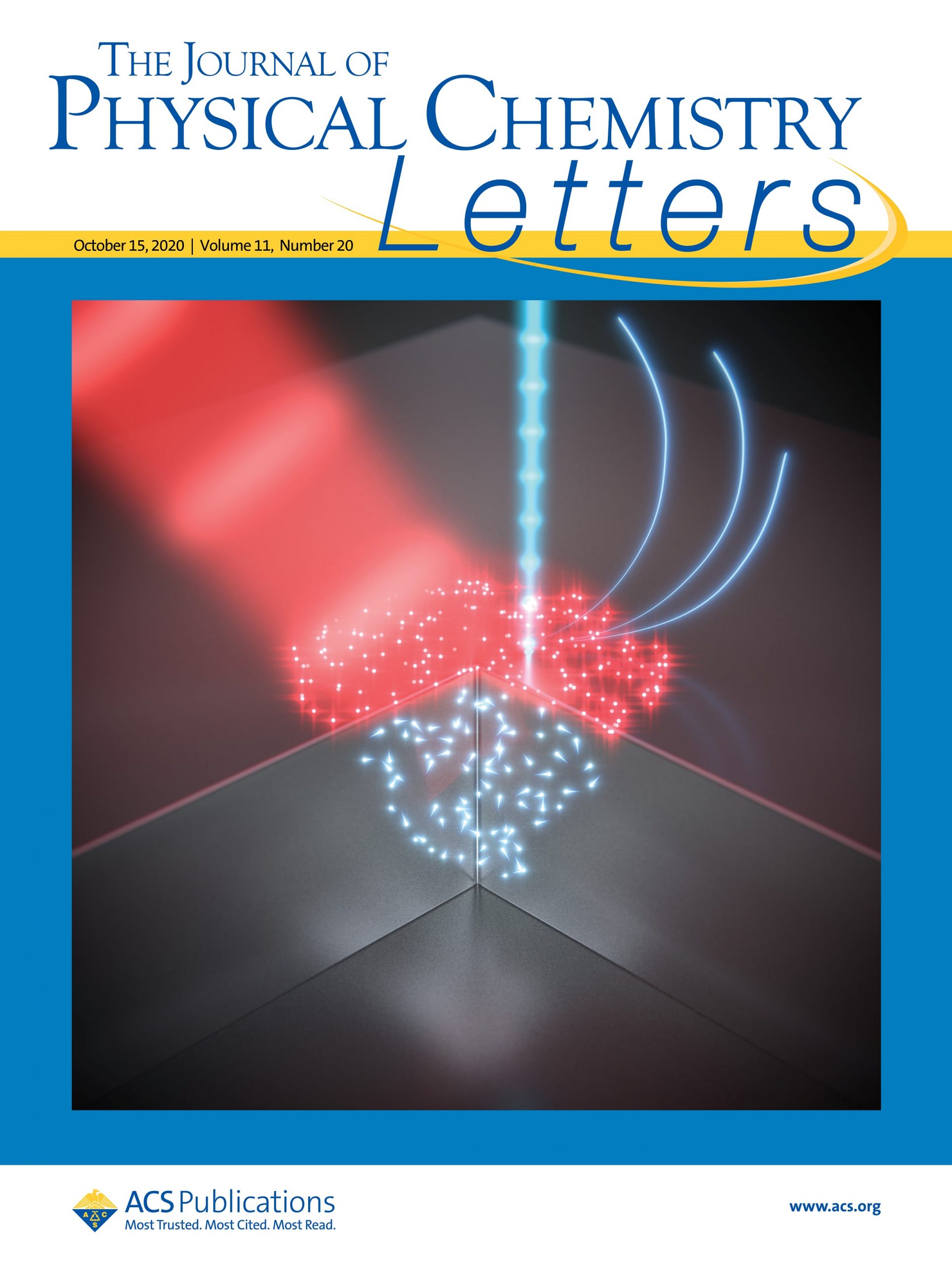
Visualizing the behaviour of charge carriers will benefit the design and functionality of semiconductor devices. This, which seems a great idea, seems equally unattainable. However, at Delft University of Technology (The Netherlands) they’re famous for not having any respect for seemingly unattainable challenges.
Jacob P. Hoogenboom et al. have developed a technique to visualize “fast bulk charge recombination and slow trapping”. These two competing processes involve fast free charges and slow, more stationary, trapped charges. The device, a Lock-in ultrafast scanning electron microscope has enabled, in a proof of concept, a deep analysis of trap states on GaAs surfaces. And as they conclude, this technique will allow the study of “carrier transport in and across heterojunctions, underneath nanostructured surfaces, or at edges or layer transitions in two-dimensional materials”.
This image we made under the close supervision of Mathijs Garming (first author of the paper), has been featured as the cover of The Journal of Physical Chemistry Letters.

