Shortening bridges

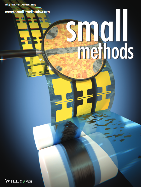
Castellanos-GĂłmez Lab is kind of obsessed with cheap production techniques of 2D materials. They’ve proved this multiple times on the past by developing imaginative ways of producing and laying 2D materials over cheap substrates or using low-cost and accessible procedures.

This time they’ve come up with a way to mechanically exfoliate van der Waals nanosheets using low cost tools. It is needless to say that this new technique shortens the distance between hardcore science and industry.

The picture that has been featured in the cover of Small Methods was made together with Carmen Munuera.

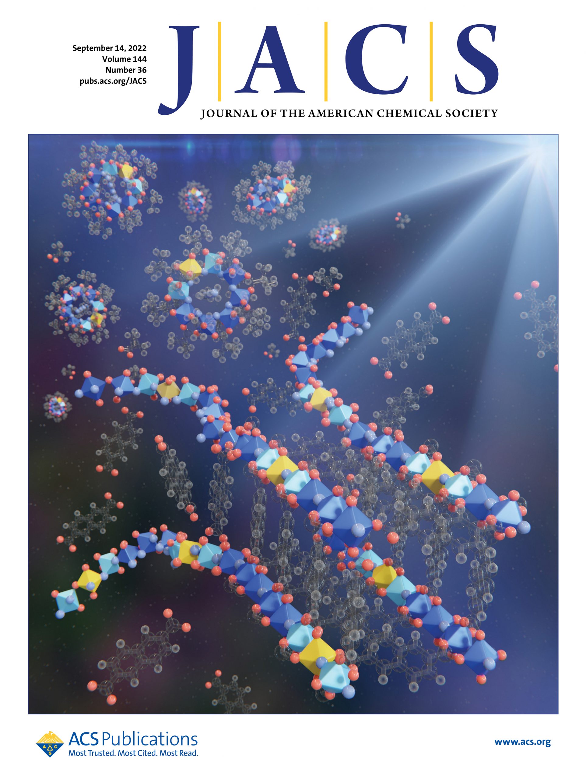
Tailoring Metal–Organic Frameworks

Felipe Gándara et al. at Materials Science Institute of Madrid has developed a new method to prepare metal–organic frameworks with specific combinations of metal elements. The funny thing (to me) is that this method reminds me of how ribosomes build proteins.

Using molecular complexes with the desired metal-atom combinations as building blocks, they’re able to synthesize these frameworks with precise atomic composition. This method will allow to increase the different ways we have now to create extremely tailored novel materials that might be used for heterogeneous catalysis or quantum computing.

Their work has been featured in the cover of JACS.

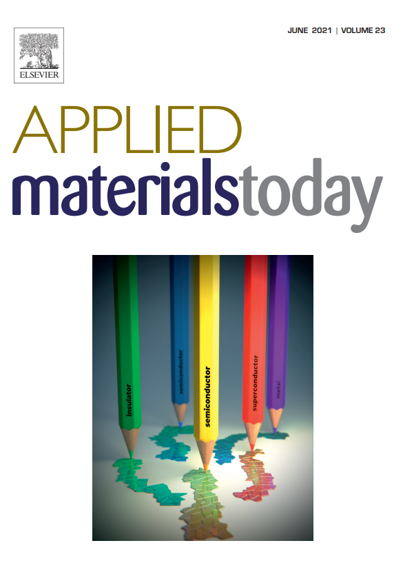
Van der Waals on paper

We’ve been talking for quite a long time about the crazy things that happen in Andres Castellanos’s Lab. And they seem to be getting crazier. The ability of this people for outside the box thinking is amazing. Actually they don’t seem to know about the box at all!

They are now working in the use of paper as a functional substrate for van der Waals materials. This materials are deposited by “simply rubbing the vdW crystals against the rough surface of paper”. The aim is to replace silicon with a cheap material. But is it paper a valid substrate? In this new work, they’ve characterized the optical and electronic properties of some of this materials in this strange new conditions. As vdW materials can behave as superconductors, insulators, semiconductors or semi-metals, researchers have to prove all these properties are maintained when transferred into paper.

And that is exactly what they did by building field-effect devices using the paper substrate as an ionic gate. This work, published in Applied Materials Today, has been featured in the cover.

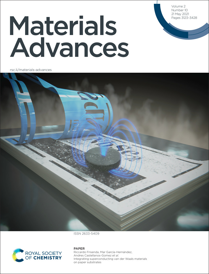
Superconductors work (on paper)

Castellano’s Lab (ICMM-CSIC) research is not only top-notch scientific work: more important, at least to me, it is funny and inspiring. They’ve also worry about the social, economic and environmental impact of technology. And we can see all that in their last paper.

Together with the Kavli Institute of Nanoscience (TuDelft) they’ve proved that it is possible to have a working van der Waals superconductor deposited on regular paper as opposed to crystalline silicon. In particular, they’ve reported the observation of  Meissner effect and resistance drop to zero-resistance state at low temperatures. As they point out, regular paper is 10.000 times cheaper that crystalline silicon. And being this technique scalable, it could have a major effect on the production of magnetic field shielding or superconducting high frequency filters.

We collaborated with them in the production of this picture that has been featured in the cover of Materials Advances.

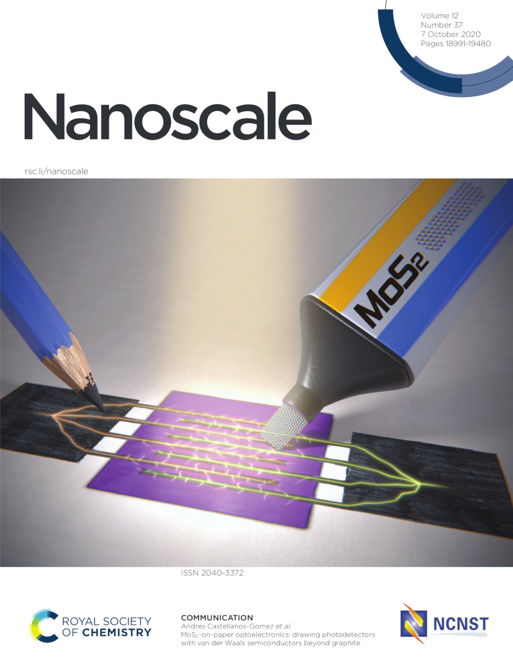
Optoelectronics: MoS2 on canvas.

If I understand it correctly (and I’m probably not), Andres Castellanos is not only making interesting discoveries in condensed matter physics. He and his collaborators (Kavli Institute of Nanoscience and the University of Teheran) are also actively working on making it easier for others to make advances on this area. How? By making easier to use, cheaper technology.

A good example is their “under 100 bucks probe station”. Another one is this recent paper where they fabricate paper-supported semiconducting devices by painting on them with MoS2 crystal. Let me repeat this last statement: BY PAINTING ON THEM WITH MoS2. They’ve not only proved this methodology works and produces perfectly working devices. They also show how this approach could open the path for the construction of cheaper sensors.

The picture we did for them to illustrate this process has been featured in the cover of Nanoscale.

Hedgehog spin textures

Magnetic skirmions are quasiparticles which present extended configurations (or textures) of spins and their physics are of great interest since they could be used in spintronics as sensors or memory storage devices. Its manipulation and tailoring is thus of great importance.
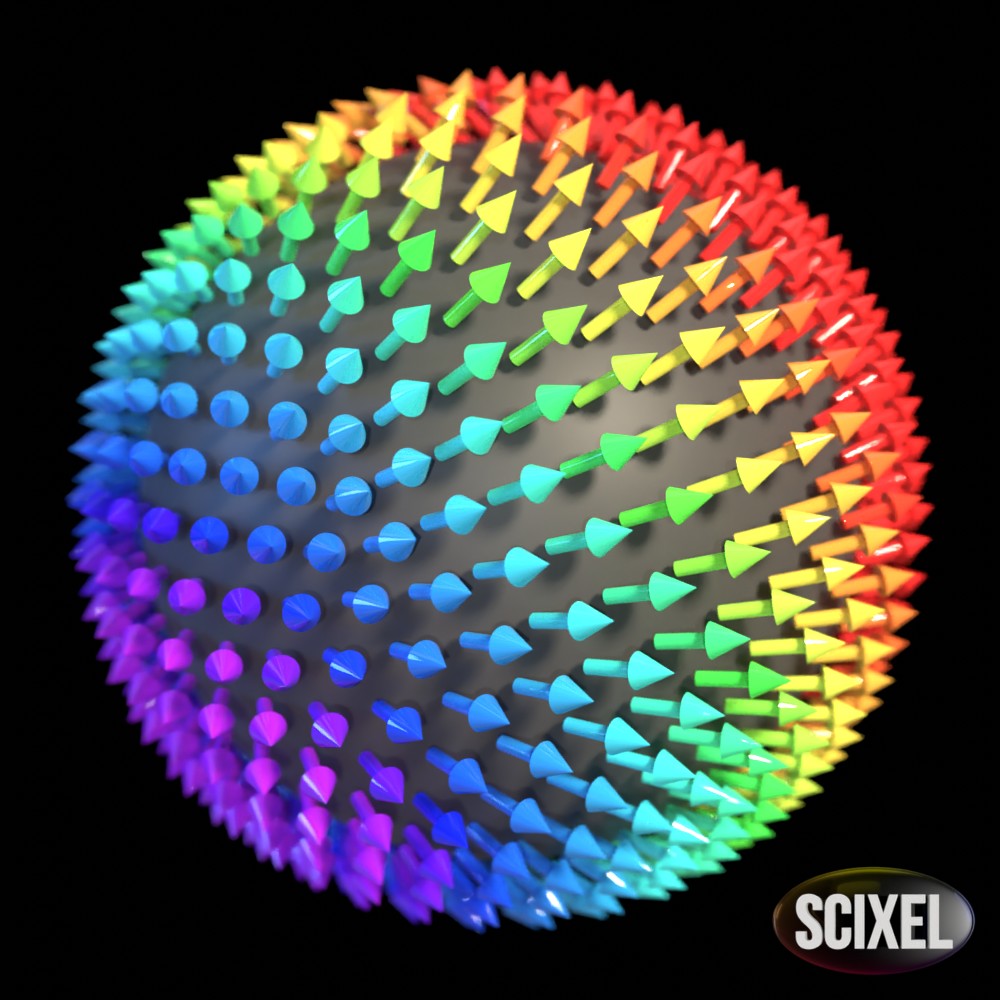
In a recent work published in Nanoscale, a group led by Prof. Agustina Asenjo, report the stabilization of half hedgehog skyrmionic configuration in permalloy hemispherical nanodots, induced by the stray field of the MFM probe.

As the first author, Eider Berganza, explains, “this is a remarkable achievement due to soft magnetic nature of the permalloy and the absence of the choice of the material, which does not present magnetocrystalline anisotropy or Dzyaloshinskii–Moriya interaction, considered as necessary ingredients for the nucleation of skyrmions”.


This research, has been a huge collaborative effort that involved sample preparation, measurements and theoretical micromagnetic simulations in Spain, Germany and the US.
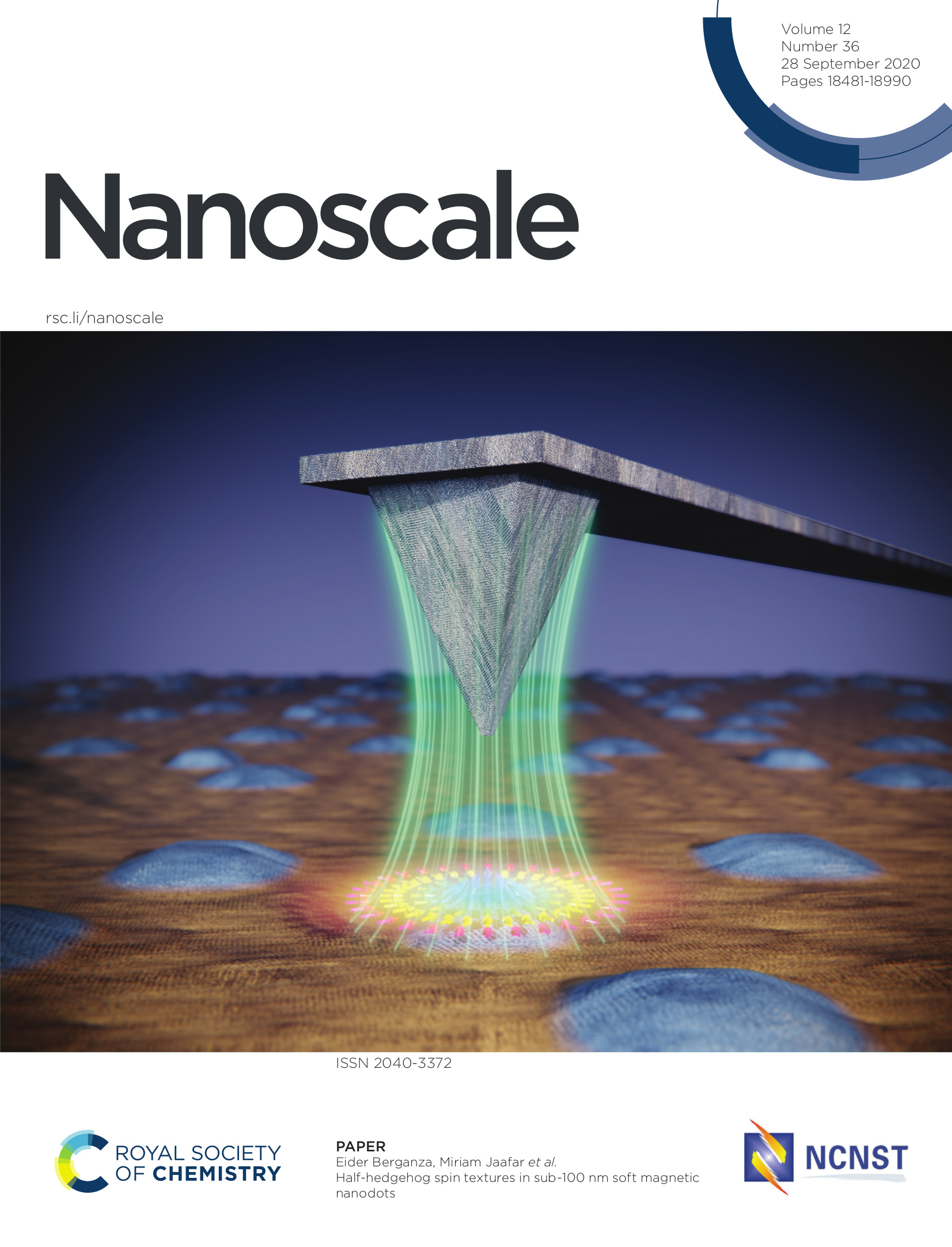
This image we did under the supervision of Eider Berganza and Miriam Jaafar (ICMM-CSIC) has been featured in the Cover of Nanoscale. Personally, has been the apex of a long and beautiful collaboration with old friends.
 

A strain tunable single-layer MoS2 photodetector

Lets take a single layer of MoS2. Lets attach it to a surface in such a way that it can be stretched (or compressed) and there you have it: A strain tunable single-layer MoS2 photodetector. A device which uses strain to change the electrical and optical properties of 2D materials. In particular they’ve proven that with this method, they can reversibly change the photoresponsivity, the response time and the spectral bandwidth of single layered MoS2.

At Dr. Castellanos Lab, they are excelling at beautiful and elegant research. “… we demonstrated that applying tensile biaxial strain to the MoS2 device can be an effective strategy to increase both the responsivity and the wavelength bandwidth of the photodetector (at the expense of a slower response time), while compressive strain can be exploited to yield faster photodetectors (although with a lower photoresponse and with a narrower wavelength bandwidth). This adaptable optoelectronic performance of this device can be very useful to adjust the photodetector operation to different lighting conditions, similarly to human eye adaptability (scotopic vision during the night vs. photopic vision during the daylight).

Their research is a collaboration between ICMM-CSIC, Imdea Nanociencia and the State Key Laboratory of Tribology, Tsinghua University, Beijing and has been recognized with the inner cover of Materials Today.

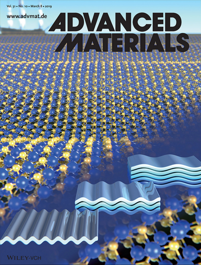
Waves and Stress

Measuring the mechanical strength of a material at the nanoscale is challenging . If the object we are measuring happens to be a two-dimensional material, the task amazingly difficult. But people at Castellanos-GĂłmez Lab are really smart. They’ve adapted a method (already used with organic thin films) to determine these materials Young Modulus that, apart from other advantages, does not require the material to be freely suspended.

To make a long story short, they compress the material. Not been freely suspended, ripples appear all over the material. The wavelength of this ripples depends only in the elastic properties of the film and the substrate, so voilĂĄ! Frankly, much easier to explain than to perform.

These results were published in Advanced Materials.

To illustrate it, and requested by Dr. Andrés Castellanos-Gómez, we did this image that made it to the back cover of Advanced Materials.

NanoCosmos: the beginning

About 4 years ago Prof. Jose Ángel MartĂ­n Gago approached me to talk me about the NANOCOSMOS project. As they explain in their website, “NANOCOSMOS will take advantage of the new observational capabilities (increased angular resolution) of the Atacama Large Millimeter/submillimeter Array (ALMA) to unveil the physical and chemical conditions in the dust formation zone of evolved stars”.  Simply put, they are studying the debris stars create and the role this dust plays in the life/death recycling story of the universe.

This is a huge ERC funded project directed by Prof. José Cernicharo which has put together research groups from Spain and France.

And this is where Natalia Ruiz Zelmanovitch (Public Information Officer of the project) appears. She happens to be the most-committed-with-outreach-and-dissemination-of-science I’ve ever met. And she wants to tell the story of the NANOCOSMOS project. And she wants to tell it right.

She is behind the production of “NANOCOSMOS: un viaje a lo pequeño.” Here you can watch the trailer:

Scixel has been in charge of the 3D visualizations of the space: stars, nebulae, galaxies and planetary systems. We have been working with the Nanocosmos people for a few years now and I can tell you, if I know Natalia enough, this is just the beginning. So, stay tunned!

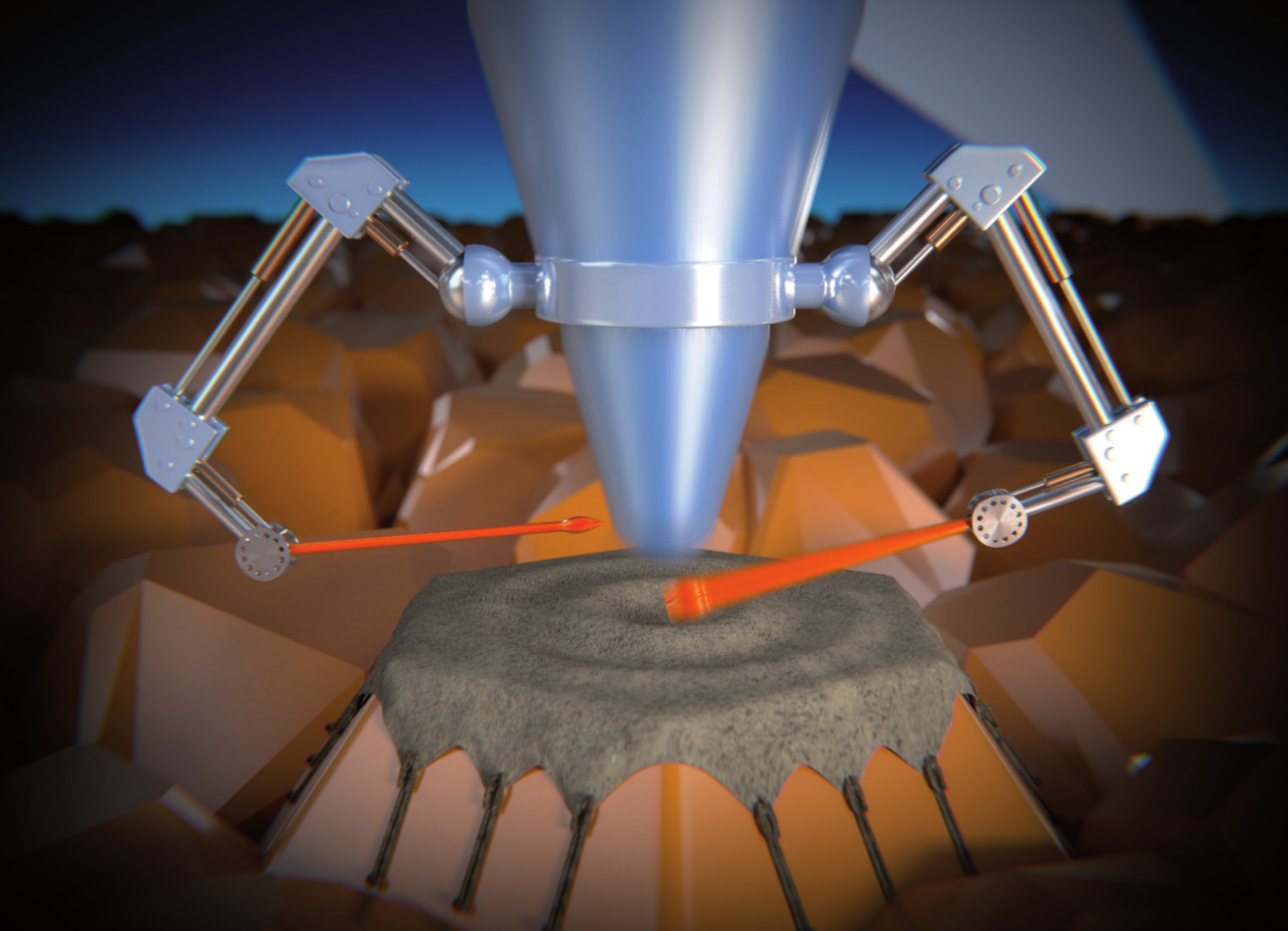
Mapping stress at the nanoscale

Stress is the main cause of failure in mechanical and electronic devices incorporating thin films. At the same time, our knowledge of stress at the nanoscale, happens to be very limited and one of the reasons is that we have no access to the measurement of stress at this tiny scale.

And this is what Celia Polop, Enrique Vasco, Alma P. Perrino and Ricardo GarcĂ­a (Universidad AutĂłnoma de Madrid and Material Science Institute of Madrid-CSIC) have solved. They’ve just presented a novel method to map stress on surfaces with a sub 10nm resolution. This method, supported by finite element simulations, has allowed them to map stress on polycrystalline gold films.

We made this image (featured in Nanoscale) illustrating their work, strongly supported by Enrique Vasco and Celia Polop.