If I understand it correctly (and I’m probably not), Andres Castellanos is not only making interesting discoveries in condensed matter physics. He and his collaborators (Kavli Institute of Nanoscience and the University of Teheran) are also actively working on making it easier for others to make advances on this area. How? By making easier to use, cheaper technology.
A good example is their “under 100 bucks probe station”. Another one is this recent paper where they fabricate paper-supported semiconducting devices by painting on them with MoS2 crystal. Let me repeat this last statement: BY PAINTING ON THEM WITH MoS2. They’ve not only proved this methodology works and produces perfectly working devices. They also show how this approach could open the path for the construction of cheaper sensors.
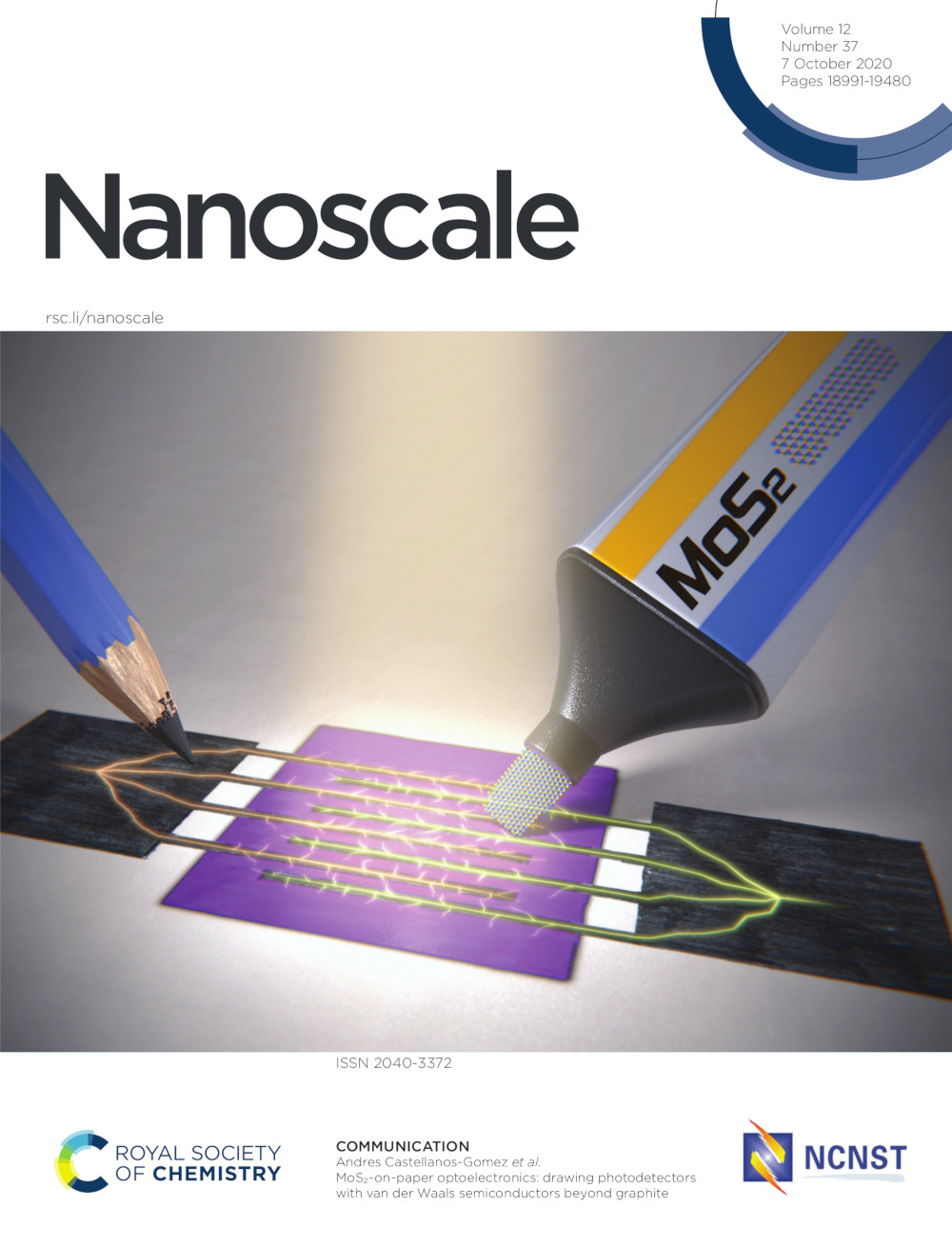
The picture we did for them to illustrate this process has been featured in the cover of Nanoscale.