Field Effect, now in 2D!

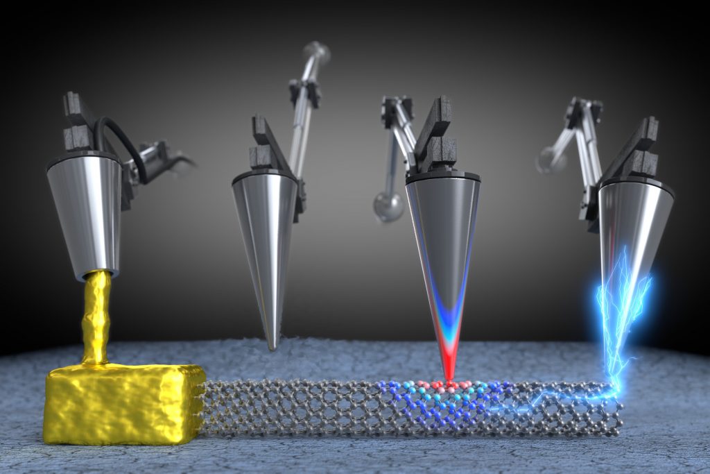
Despite his age, Dr. Mario Lanza has a long experience and deep knowledge on the physics and development of micro and nanoelectronic devices. In this recent article he an his coworkers discuss “the main challenges and potential solutions towards the fabrication of field effect transistors with 2D semiconducting channels”. In particular, there is a useful analysis on how this technology, now dealing with sizes that approach the interatomic distances, could be implemented in the current semiconductor industry.

This picture we did for him was featured on the cover of Advanced Functional Materials.

Swiss Army SPM

Mario Lanza proposes a new scanning probe microscopy technique that can examine local phenomena, and conductive atomic force microscopy, in particular, study local electromechanical properties. Check it in Nature Electronics!

In this schematic illustration we did to illustrate his proposition, it is shown how this setup, would allow multiple experiments to be carried out simultaneously and under vacuum conditions.


Do electric neurons dream of…

This is getting out of hand. At LanzaLab they try to emulate the behavior of neuron synapses using multilayered hexagonal boron nitride (h-BN) . An interesting paradigm states that a biologically inspired computing architecture, will overcome the energy and efficiency limitations of classic computing architectures. To carry it out will require the design of electronic neurons and synapses. There are several features to be copied from mother’s nature design: it has to be fast, energetically efficient and it has to have a long term/short term plasticity. And at Lanzalab, they’ve achieved most of them. Their h-BN devices consume between 0.1 fW and 600 pW and they have a truly fast response: around 10ns.

We made this image supervised by Prof. Mario Lanza to illustrate their work published in Nature Electronics.