Mapping stress at the nanoscale

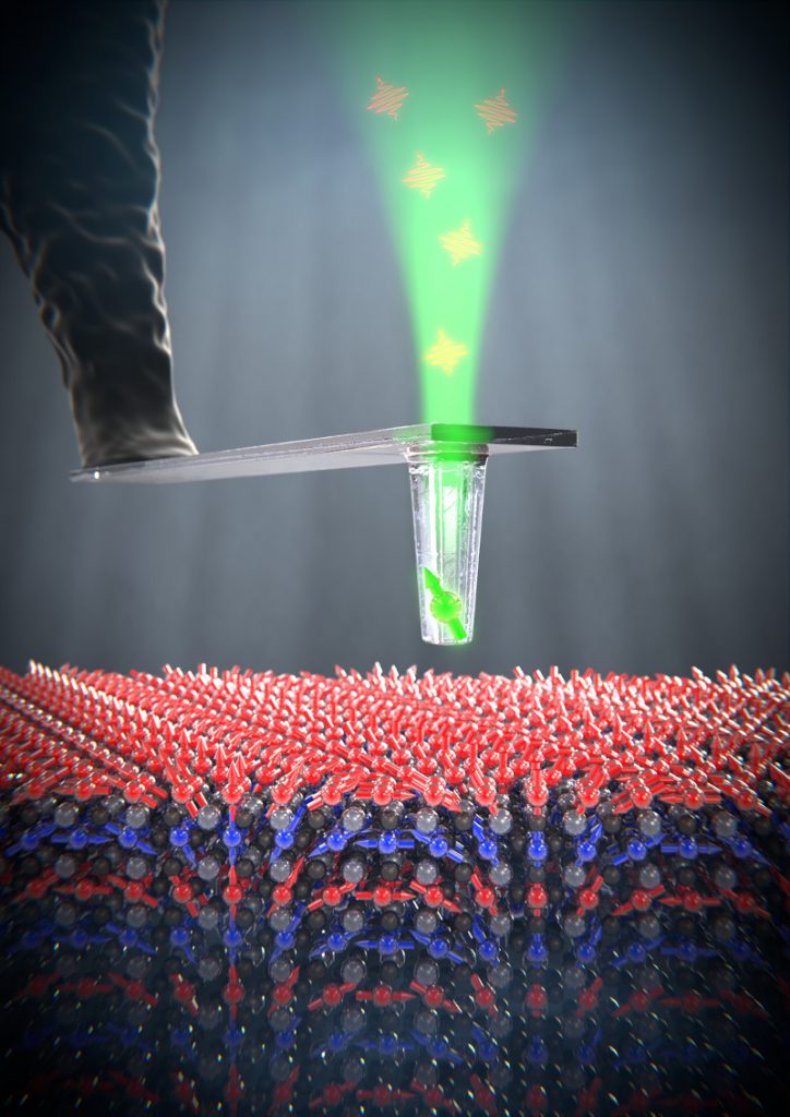
Stress is the main cause of failure in mechanical and electronic devices incorporating thin films. At the same time, our knowledge of stress at the nanoscale, happens to be very limited and one of the reasons is that we have no access to the measurement of stress at this tiny scale.

And this is what Celia Polop, Enrique Vasco, Alma P. Perrino and Ricardo García (Universidad Autónoma de Madrid and Material Science Institute of Madrid-CSIC) have solved. They’ve just presented a novel method to map stress on surfaces with a sub 10nm resolution. This method, supported by finite element simulations, has allowed them to map stress on polycrystalline gold films.

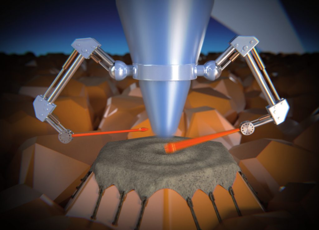
We made this image (featured in Nanoscale) illustrating their work, strongly supported by Enrique Vasco and Celia Polop.

Hidden magnetic spirals

At Quantum Sensing Lab (University of Basel) they are real experts at sensing magnetic fields. To prove it, and together with the Swiss Nanoscience Institute, the University of Montpellier and several laboratories from University Paris-Saclay they’ve just reported in Nature the visualization (in real space) of non-collinear antiferromagnetic order in a magnetic thin film at room temperature with nanometer resolution.

In particular, they’ve scanned Bismuth ferrite showing that exhibits a spiral magnetic ordering, with two superimposed electron spins. This might be particularly suitable for data storage devices because these materials magnetic fields can be easily modified using electric fields.

We did this image with the help of Prof. Patrick Maletinsky.

Light memories

Simply put, professors Philipp Treutlein, Richard Warburton et al (University of Basel), had built a memory that stores photons. That’s it. They’ve just proved that it is possible to “write” by storing the photons in an atomic vapor and also to “read” them out, without dramatically changing their quantum state.

If you know something about quantum physics, you’ll understand how amazingly challenging this is. And if you don’t, let’s just say that the event has received some attention

A quantum photon-based memory is one of the pillars of future quantum network technology. Such a device will bring faster and safer communications. And interestingly, the novel Basel approach is particularly simple, not requiring cooling devices or complex vacuum systems. This research has been published in Physical Review Letters.


Really honored to be contacted by them (again) we did this picture, closely advised both technically and artistically by Dr. Janik Wolters, first author of the paper.

We demand more and better photons!

The development of quantum technologies requires the regular use of weird quantum effects such as quantum entanglement. And the regular use of entanglement requires the use of coherent spins and coherent photons. Maybe the best host of coherent spins are nitrogen vacancy (NV) centers in diamond. However, these NV centers are pretty inefficient at generating single coherent photons: only 3% of the generated emission is usable.


And then doctoral student Daniel Riedel appeared to break the storyline by dramatically increasing the efficiency of the NV centers in a 46%, also doubling the photons emission rate.  Riedel et al (Quantum Sensing Lab and Nanophotonics Group, University of Basel) have reached this achievement by placing a tiny high-quality diamond between two mirrors, spaced only a few micrometers. They also prove a 10 years old theoretical prediction… quite some stuff for a single paper… It’s difficult to predict how much impact this achievement will have eventually, but it has surely brought the implementation of quantum systems (as quantum internet) much closer.

Together we made this image to illustrate the device.

Graphene: behind the scenes

Prof. Fernández-Rossier is an interesting person for many reasons. Apart from his research work and being a Spinograph partner, he has recently started a new research center (QuantaLab). And some how he still manages to find some time for scientific outreach. And this is a good example.

Here he explains the mass production of the ubiquitous graphene.


We just helped with the video. And as a side note, we are particularly proud of the music piece.