Hyperlenses

This has been a good year for nano optics. And the research group 2DNanoptica (Oviedo, Spain) is largely responsible for this. Leading international collaborations, they’ve published two major advances in high impact factor journals during 2021.

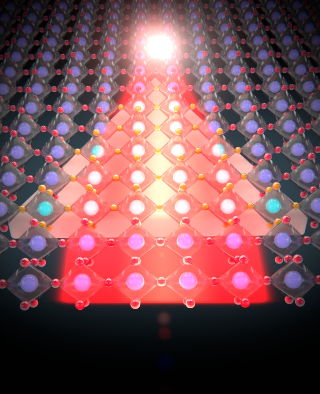
In the first one, published in Nature Communications, they’ve presented a study on the refraction of light in highly anisotropic materials at the nanoscale. They’ve shown how light shows an exotic behaviour under this circumstances: how it can propagate in non-intuitive directions or how the refracted waves can be highly confined. Using these principles, they’ve built nanometric lens able to focus light in spaces way smaller that its wavelength.
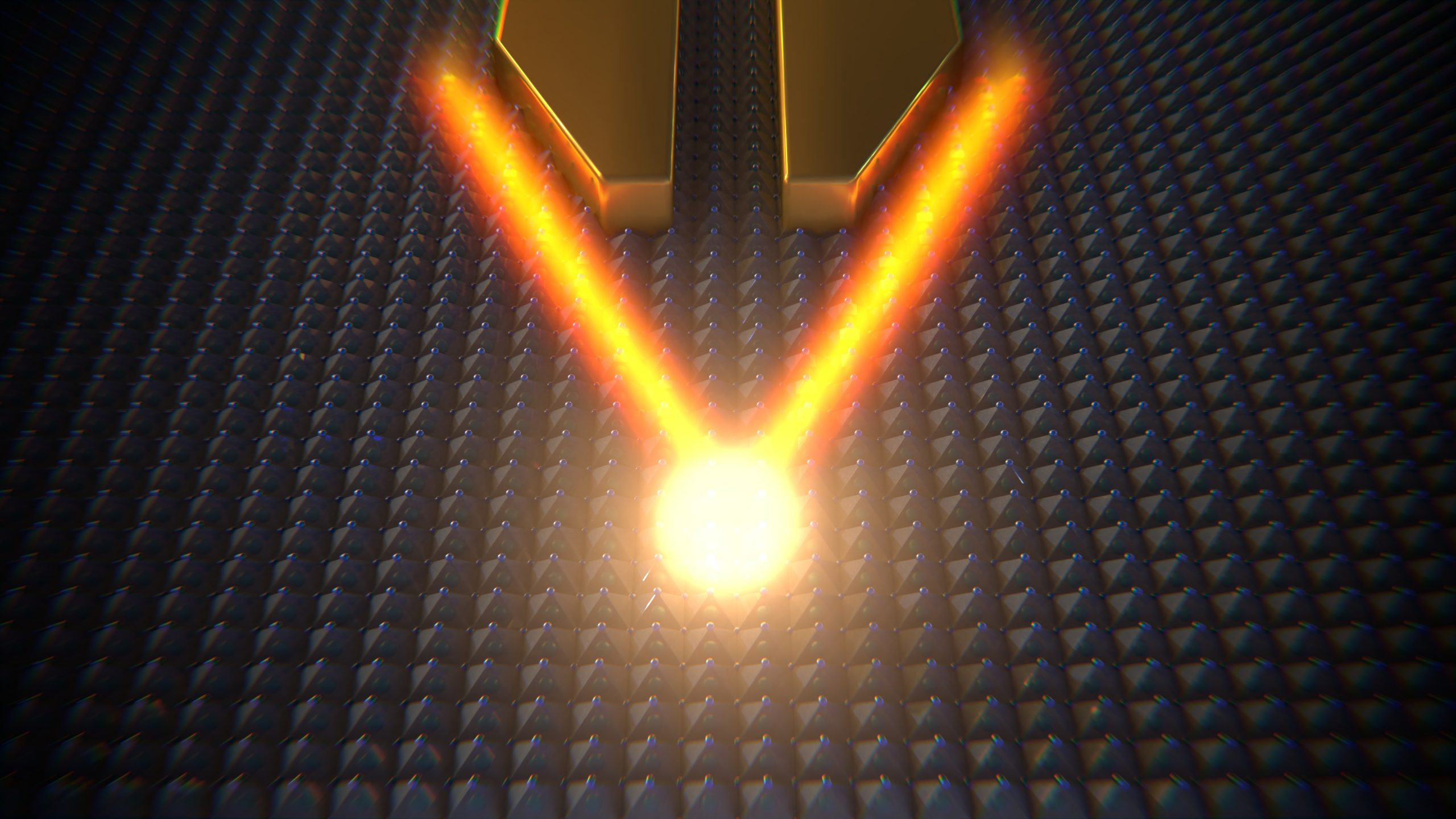
In the second one, published in Science Advances, they show a similar result, but this time using two gold nano antennas, shaped in a special way that allows to focus light with a high level of confinement.
These results have obvious applications in optical computation or communications. But also they can work as biological or atmospheric sensors. However that does not really matter, does it? Because this work (both theoretical and experimental) is just beautiful. And that should be enough.


We did this two pictures in collaboration with Patricia Bondía to illustrate this work under close supervision of Pablo Alonso-González and Javier Martín Sánchez.

Mapping energy carriers

How can we map out traps on a surface? Ferry Prins, Michael Seitz et al. have developed a curious strategy. First, they’ve injected a small population of excitons (gaussian shaped) in a 2D metal halide perovskite. The flow of these excitons through the material will be affected by the traps, kind of how the flow of water is affected by stones at the riverbed. Therefore, by visualising the flow of the excitons, you can “accurately map out the trap-state landscape in the perovskite lattice”.

This research, has been featured in the cover of Advanced Optical Materials. The picture has been done under the supervision of Ferry Prins and Michael Seitz.

Van der Waals on paper

We’ve been talking for quite a long time about the crazy things that happen in Andres Castellanos’s Lab. And they seem to be getting crazier. The ability of this people for outside the box thinking is amazing. Actually they don’t seem to know about the box at all!

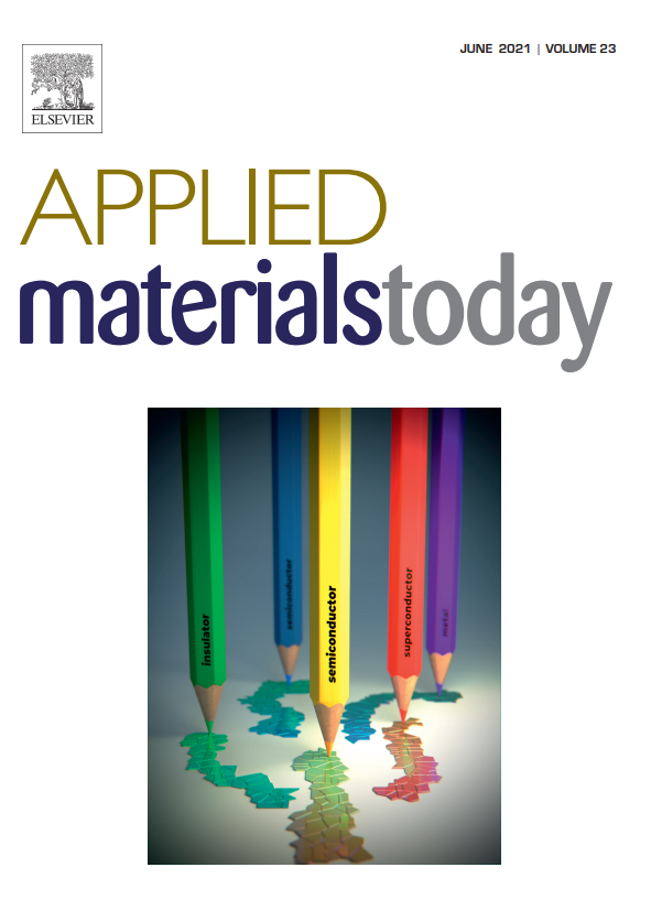
They are now working in the use of paper as a functional substrate for van der Waals materials. This materials are deposited by “simply rubbing the vdW crystals against the rough surface of paper”. The aim is to replace silicon with a cheap material. But is it paper a valid substrate? In this new work, they’ve characterized the optical and electronic properties of some of this materials in this strange new conditions. As vdW materials can behave as superconductors, insulators, semiconductors or semi-metals, researchers have to prove all these properties are maintained when transferred into paper.

And that is exactly what they did by building field-effect devices using the paper substrate as an ionic gate. This work, published in Applied Materials Today, has been featured in the cover.

Hot carriers thermalization

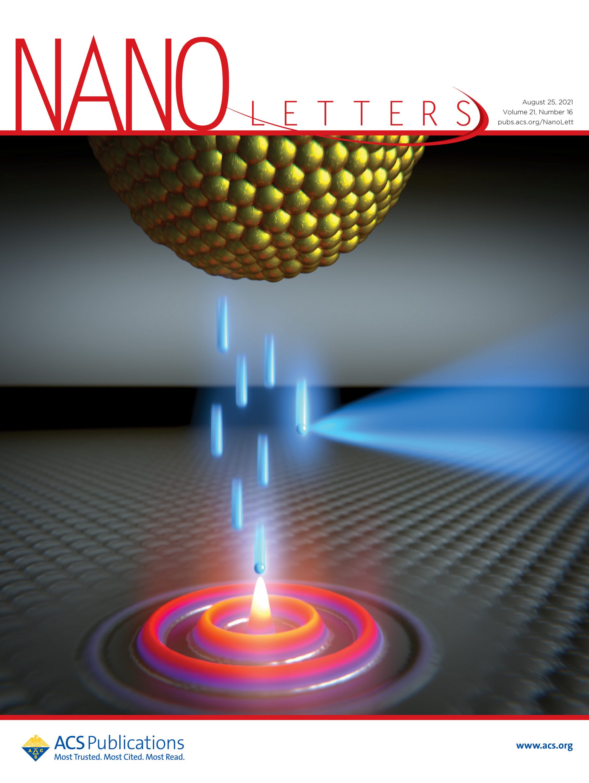
A research collaboration between IMDEA Nanociencia, DIPC and IFIMAC led by Roberto Otero has just proposed a new method to measure electronic temperatures in metallic nanostructures.

In particular, they show that the electronic temperature can be derived from “the shape of the tunnel electroluminescence emission edge in tunnel plasmonic nanocavities”.

This method, published in Nanoletters, will allow the study and understanding of the thermalization of nanoscale systems with picosecond resolution.

Osmium is the key

Ana Pizarro and colleagues are a sort of modern watchmakers to my eyes. But instead of using gears and springs, they work with atoms, bonds and molecules. They carefully tailor them to produce chemical reactions in specific places that are triggered by specific conditions. In particular, they’re putting a lot of effort in molecules that work as catalysts in the cytoplasm and are triggered by pH changes.

This time they bring to our attention this beautiful specimen: [Os(η61-C6H5(CH2)3OH/O)(XY)]+ an osmium(II) tethered half-sandwich complex that has shown to carry out transfer hydrogenation reactions inside cells in a reversible way. The particular properties of this molecule could give it a central role in cancer therapies.

This work, published in Chemical Science has been featured in the cover with this image we did together with Ana Pizarro.

Towards healthier photovoltaics.

Science is always teaching us how to do new things. But it is also important how it teach us how to do old stuff in a much better way. And with better we mean, in a faster, cleaner, healthier, more sustainable way. And that is kind of what Vincenzo Pecunia et al. do in their last paper.

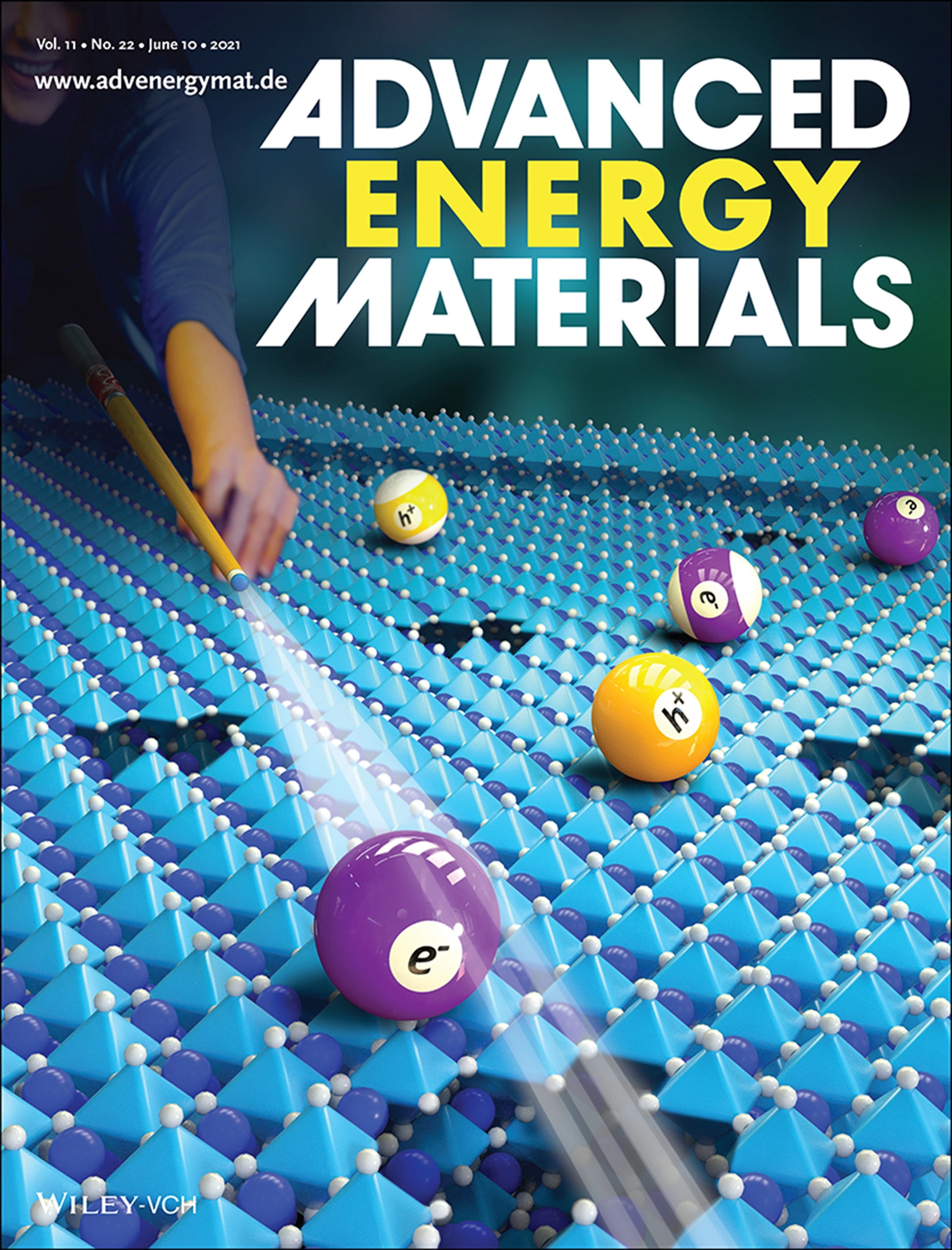
They’ve developed a technique to study the impact of defects in lead-free-perovskites inspired materials. These materials are gathering a lot of interest since they can be key to the development of green, high-performance photovoltaics. And the efficiency of these materials is closely related to their defect tolerance.

This new technique is not only highly sensitive but it is also facile and widely applicable. We did this picture together with Vincenzo Pecunia and it has been featured in the cover of Advanced Energy Materials.


Smart AFMs

Machine learning is already a thing and it is slowly percolating into the most unexpected places. AFM is its most recent victim and Juan F. Gonzalez-Martinez et al. (Biofilms-Research Center for Biointerfaces at Malmö Univerity) have put them together.

Although deep learning techniques had already been used for AFM related analysis, for the first time (to my knowledge) it’s been used to drive the microscope to locate particularities of the samples. They have used Plasmid DNA from E. coli with assubject, and the challenge was to teach the microscope to identify and distinguish single molecules and take images of them with different lateral resolutions.

Although this type of studies is not technically challenging, doing them is extremely time consuming because it needs the close supervision of the researcher. Thus, this breakthrough could open the door not only to a full autonomous AFM but to the analisys of large amounts of samples and statistically significant studies.

We did this picture (featured in the inside cover of Nanoscale) together with Javier Sotres, first author of the paper.


Superconductors work (on paper)

Castellano’s Lab (ICMM-CSIC) research is not only top-notch scientific work: more important, at least to me, it is funny and inspiring. They’ve also worry about the social, economic and environmental impact of technology. And we can see all that in their last paper.

Together with the Kavli Institute of Nanoscience (TuDelft) they’ve proved that it is possible to have a working van der Waals superconductor deposited on regular paper as opposed to crystalline silicon. In particular, they’ve reported the observation of  Meissner effect and resistance drop to zero-resistance state at low temperatures. As they point out, regular paper is 10.000 times cheaper that crystalline silicon. And being this technique scalable, it could have a major effect on the production of magnetic field shielding or superconducting high frequency filters.

We collaborated with them in the production of this picture that has been featured in the cover of Materials Advances.

Superconducting graphene

Graphene’s business card is running out of space. We’ve already seen it doing nearly every possible thing in condensed matter physics. And superconductivity was to be there. It was a matter of time.

Magnetism and superconductivity don’t get along… to put it politely. So when you add magnetic atoms into a superconductor, the superconducting order is locally broken and spectral features (called Yu-Shiba-Rusinov states) appear inside the superconducting gap. And this features are important because they might be useful for quantum computing. 

Ivan Bruhuega, has lead an important research collaboration involving several countries (Finland, France, Portugal and Spain), that has for the first time observed these Yu-Shiba-Rusinov states in graphene. The complexity of this experiment is hard to grasp. To begin with, you have to induce superconductivity in graphene. They’ve done this by growing nanometer scale superconducting Pb islands over it. And then, using scanning tunneling microscopy and spectroscopy they’ve visualized Yu-Shiba-Rusinov states in the graphene grain boundaries. Quite a challenge.

We made this picture to illustrate the experience and it’s been featured in the cover of Advanced Materials.

Atomic dialogues

Here I bring you another scientific milestone performed in TUDelft and published in Science. This time is about single atoms exchanging quantum information and in the way, unveiling quantum mechanics at a fundamental level. Veldman et al. have been spying single magnetic atoms and they’ve observed their reaction when one of their neighbours received an electric pulse. And this is not an easy task.

First, Sander Otte’s team has to built this “neighbourhood” of atoms by placing them close to each other at a distance at which they’re able to “feel” each other’s magnetic moments. And then the fun part starts: they send a pulse at one of the atoms and observe its neighbour’s reaction. This starts a sort of a conversation between the two atoms, an interchange of quantum information. A kind of a dance in which the two atoms swap their magnetic moment back and forth.

This observation has some interesting implications: first, it means another step in the understanding of qbits. But the inherent violence of the process (this aggressive non-coherent electric pulse) could mean that we might not need to be so careful at initializing quantum states.

To illustrate this conversation we made this picture under the close supervision of Prof. Sander Otte.