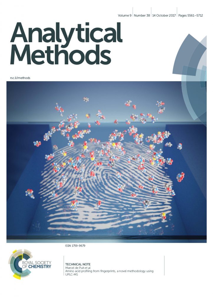
About 4 years ago Prof. Jose Ángel Martín Gago approached me to talk me about the NANOCOSMOS project. As they explain in their website, “NANOCOSMOS will take advantage of the new observational capabilities (increased angular resolution) of the Atacama Large Millimeter/submillimeter Array (ALMA) to unveil the physical and chemical conditions in the dust formation zone of evolved stars”. Simply put, they are studying the debris stars create and the role this dust plays in the life/death recycling story of the universe.
This is a huge ERC funded project directed by Prof. José Cernicharo which has put together research groups from Spain and France.
And this is where Natalia Ruiz Zelmanovitch (Public Information Officer of the project) appears. She happens to be the most-committed-with-outreach-and-dissemination-of-science I’ve ever met. And she wants to tell the story of the NANOCOSMOS project. And she wants to tell it right.
She is behind the production of “NANOCOSMOS: un viaje a lo pequeño.” Here you can watch the trailer:
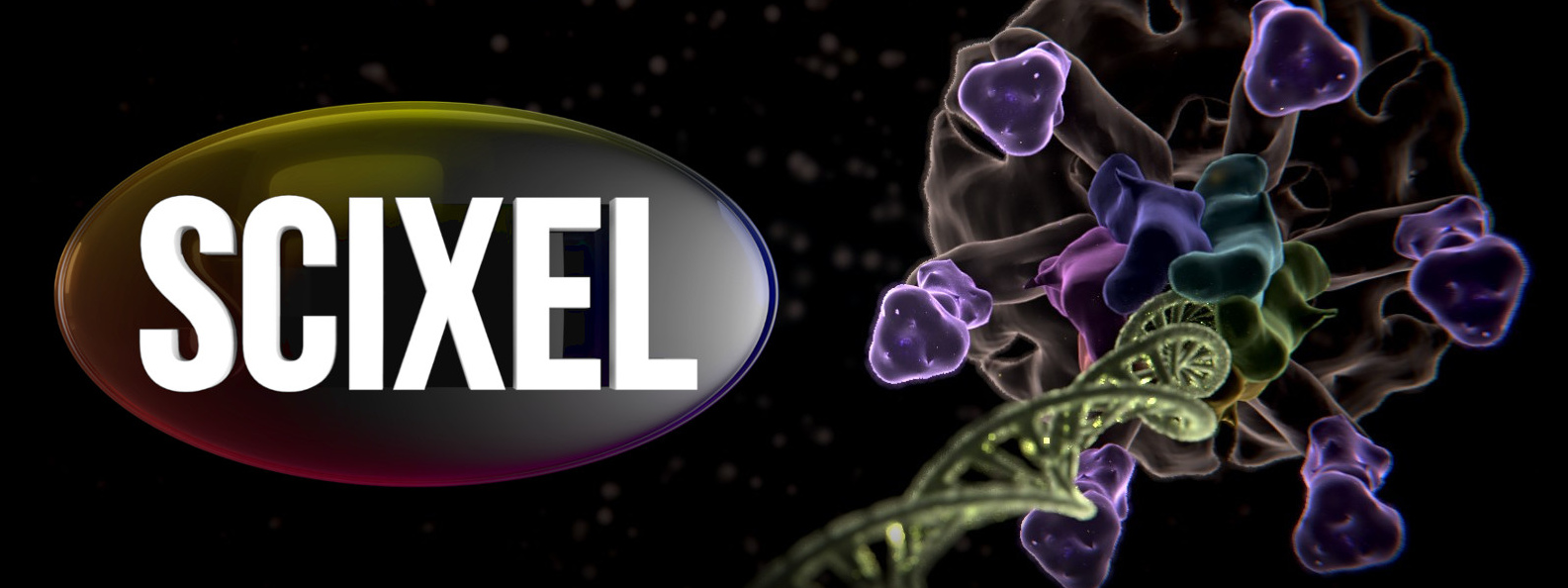
Scixel has been in charge of the 3D visualizations of the space: stars, nebulae, galaxies and planetary systems. We have been working with the Nanocosmos people for a few years now and I can tell you, if I know Natalia enough, this is just the beginning. So, stay tunned!