Stress is the main cause of failure in mechanical and electronic devices incorporating thin films. At the same time, our knowledge of stress at the nanoscale, happens to be very limited and one of the reasons is that we have no access to the measurement of stress at this tiny scale.
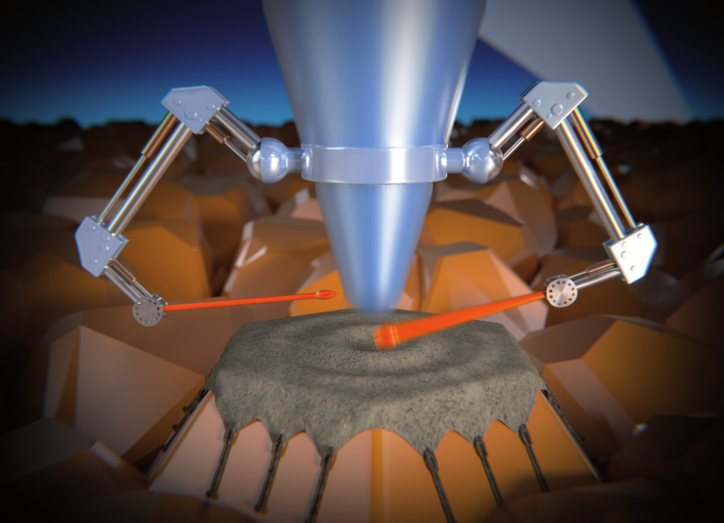
And this is what Celia Polop, Enrique Vasco, Alma P. Perrino and Ricardo García (Universidad Autónoma de Madrid and Material Science Institute of Madrid-CSIC) have solved. They’ve just presented a novel method to map stress on surfaces with a sub 10nm resolution. This method, supported by finite element simulations, has allowed them to map stress on polycrystalline gold films.
We made this image (featured in Nanoscale) illustrating their work, strongly supported by Enrique Vasco and Celia Polop.

