Good Vibrations

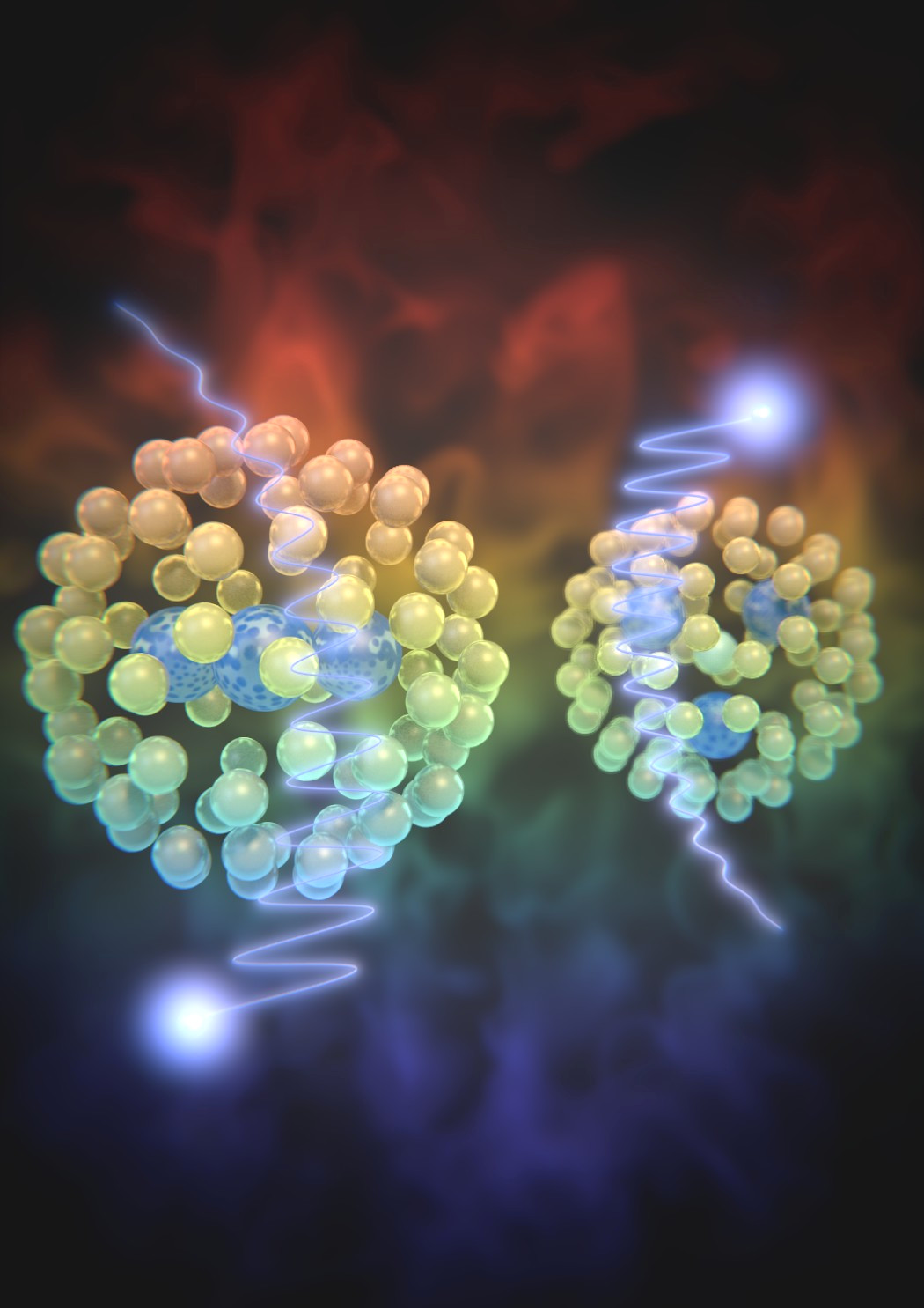
Today we want to talk about light and molecular vibrations coupling. It is known that infrared light can interact with matter through the molecules natural vibrations. What it was not so well known is that this coupling between light and matter can be so strong that it can change the material properties. But this strong-coupling-landscape has yet to be explored.

Researchers from CIC nanoGUNE BRTA (San Sebastian, Spain), the Donostia International Physics Center (San Sebastián, Spain) and the University of Oviedo (Spain) have employed a spectroscopic nanoimaging technique to achieve this strong coupling. By using “a particularly strong compression of infrared light” and a “thin layer of hexagonal boron nitride” they’ve explored in real space “how the phonon polaritons couple with the molecular vibrations” of organic molecules.

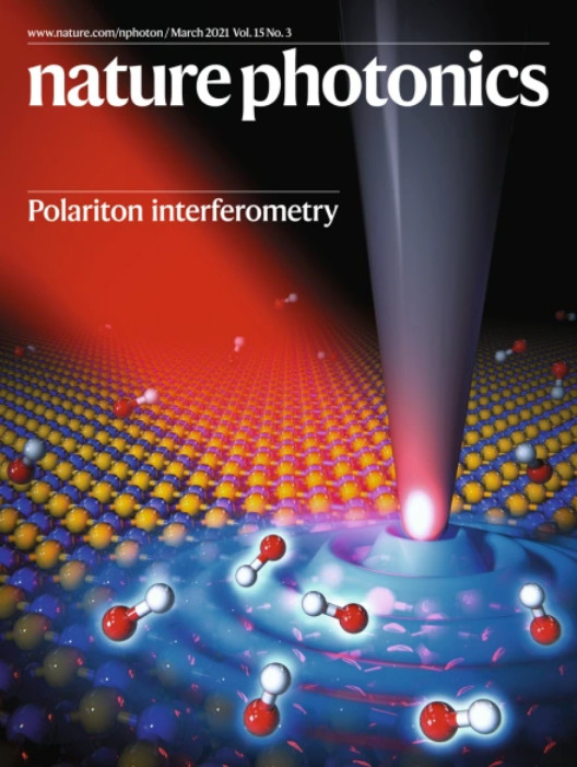
Their findings, published in Nature Photonics could have an impact in molecules detection technologies but more importantly, it opens a door to the study of quantum aspects of strong vibrational coupling.

This picture we did under the supervision of Andrei Bylinkin (first author) has been featured in the cover of Nature Photonics.

Boosting our batteries

Up to this point we’ve all recognized graphene’s omnipotence. This time we bring it to the website in its role of “energy storage enhancer”. At CIC energiGUNE, Daniel Carriazo et al., have just shown how functionalizing  graphene with phosphate groups in lithium-ion capacitors, highly improves both their power but more interestingly, they cyclability.

This picture, made under the supervision of Daniel Carriazo, has appeared as the cover feature at Batteries and Supercaps.

A sustainable Internet of Things ecosystem

A future of wireless self‐powered devices is upon us. The number of sensors and devices in our close environment is growing fast. And so does its energy demand.


In his last paper, Vincenzo Pecunia proposes the use of indoor photovoltaics: a clean sustainable way to fulfill this demand with lead‐free (and thus, non toxic) perovskite‐inspired materials. In particular Pecunia and co-workers, have studied two materials, BiOI and Cs3Sb2ClxI9‐x which happen to be really bad at harvesting sun light but present high efficiencies under indoor light conditions.

This research opens a door to the study of more efficient, non-toxic perovskite‐inspired materials and a sustainable future.

Under close supervision of Dr. Pecunia we made this picture that has been featured as the cover of Advanced Energy Materials.


Single-molecule junctions and atomic contacts

Dr. Laura Rincón made her thesis defense in August 2009. The manuscript, titled Conductance, thermopower and thermal conductance measurements in single-molecule junctions and atomic contacts, is a study on the properties of these contacts in the context of molecular electronics and thermoelectricity. The defense was recently awarded with the Best Experimental Thesis GEFES award.

Dr. Rincón used this picture we made years ago on request of her PhD advisor Prof. Nicolás Agrait.

Invoking Spin Waves into the real world

Magnetic resonance imaging (MRI) has long been used as a non invasive detection technique in scientific research, industry and medicine. However, its low resolution (in the order of millimeters) makes it useless for nanotechnology applications despite its huge potential.

And this is were researchers from TU Delft, Leiden University, Tohoku University and the Max Planck Institute come into play. They’ve recently developed an MRI-like technique able to imaging magnetic waves with sub-micron resolution. Among its capacities, it is able to imaging spin waves through opaque materials such as the metal wiring on a chip. And also, it has the sensitivity to detect spin waves in magnets that are only a single atom thick. This work has been published in Science Advances.

If you’ve read my posts, you’ll know I don’t usually value my own images. But in this occasion I have to. This might be the most elegant picture I’ve made up to date. And for that, I have to thank the direction of Iacopo Bertelli and Toeno Van der Sar.


One electron at a time, please

There is plenty of room at the bottom. Well, plenty, yes, but not infinite. There is a limit on how small we can build things, or something that happens to be of great technological importance: how faint an electrical current can be. And we might have just found an answer to that.

Researchers from the Max Planck Institute for Solid State Research in Stuttgart, Ulm University and the Autonomous University of Madrid, have found the most basic way of producing an electrical current. They’ve coupled two atomic energy levels and then measured the electronic transference between them, one electron at a time. We’re talking about single electrons here, folks! As it can be imagined, this presents a huge challenge: a fine tunned scanning tunneling microscope, low temperatures, crazy stability, pure skill in the sample preparation, etc. You can read the paper published in Nature Physics, or a more comprehensive explanation here.

In science we know how sterile it is to discuss the possible technological breakthroughs this research can bring. But this is of no importance here, because this research is just beautiful, and that is enough. This is about witnessing the quantum world at its most basic form, without ornaments. Do you know these simplistic pictures of energy levels with a wavy line connecting them? These people have made that picture real.

And talking about pictures, we made this one on request of Dr. Christian Ast and Prof. Carlos Cuevas, to illustrate not the experiment, but how they feel about it. And as an illustrator, that’s also beautiful.

The Third Daughter

We’ve started a new project called The Saga of the Third Daughter, a series of videos telling the story of the Great Oxidation Event. Interestingly, or so we think, these videos are not designed to be part of an outreach project. We wanted to tell this story as if it was a classic creation myth.

Sadly, for the moment, the videos will be only in Spanish, although an English voice over would be an option in the future.

Here we present the first Book, hope you like it!

You can check the following releases here. Also, in the website we “translate” the poetry of the tale and explain the real story in which the saga is base.

Visualizing charges

Visualizing the behaviour of charge carriers will benefit the design and functionality of semiconductor devices. This, which seems a great idea, seems equally unattainable. However, at Delft University of Technology (The Netherlands) they’re famous for not having any respect for seemingly unattainable challenges.

Jacob P. Hoogenboom et al. have developed a technique to visualize “fast bulk charge recombination and slow trapping”. These two competing processes involve fast free charges and slow, more stationary, trapped charges. The device, a Lock-in ultrafast scanning electron microscope has enabled, in a proof of concept, a deep analysis of trap states on GaAs surfaces. And as they conclude, this technique will allow the study of “carrier transport in and across heterojunctions, underneath nanostructured surfaces, or at edges or layer transitions in two-dimensional materials”.

This image we made under the close supervision of Mathijs Garming (first author of the paper), has been featured as the cover of The Journal of Physical Chemistry Letters.

Long live the Nucleobase!

Multiple medical and biological sensors and targeted drug delivery are based in the functionalization of nanoparticles (NPs) with biomolecules. The role of the NPs is to enhance the optical response of the target surroundings. But this enhancement comes with a huge risk: this same radiation can severily damage DNA or RNA producing mutations.

Johannes Feist (UAM) together with groups from the University of Modena and the University of Munich, have studied in which conditions these NPs can act as a protection for the biomolecules (in this case Uracil) while being effective in their sensing/therapeutic function. And importantly, the results proposed in their research can be easily implemented with the current nanophotonic technology.

This paper, published in the Journal of Physical Chemistry Letters, has been recognized with the cover we designed together with the supervision of Dr. Feist.

Optoelectronics: MoS2 on canvas.

If I understand it correctly (and I’m probably not), Andres Castellanos is not only making interesting discoveries in condensed matter physics. He and his collaborators (Kavli Institute of Nanoscience and the University of Teheran) are also actively working on making it easier for others to make advances on this area. How? By making easier to use, cheaper technology.

A good example is their “under 100 bucks probe station”. Another one is this recent paper where they fabricate paper-supported semiconducting devices by painting on them with MoS2 crystal. Let me repeat this last statement: BY PAINTING ON THEM WITH MoS2. They’ve not only proved this methodology works and produces perfectly working devices. They also show how this approach could open the path for the construction of cheaper sensors.

The picture we did for them to illustrate this process has been featured in the cover of Nanoscale.